Lithography Equipment Market Size, Share, Trends, Growth and Forecast 2032

Lithography Equipment Market By Type (EUV and DUV), By Technology (ArF Scanners, KrF Steppers, i-line Steppers, ArF Immersion, Mask Aligners and Others), By Application (Advanced Packaging, LED, MEMs and Power Devices), By Packaging Platforms (3D IC, 2.5D Interposer, Wafer Level Chip Scale Packaging (WLCSP), FO WLP Wafer, 3D WLP and Others) and By Region - Global and Regional Industry Overview, Market Intelligence, Comprehensive Analysis, Historical Data, and Forecasts 2024 - 2032
| Market Size in 2023 | Market Forecast in 2032 | CAGR (in %) | Base Year |
|---|---|---|---|
| USD 24.7 Billion | USD 47.3 Billion | 7.5% | 2023 |
Lithography Equipment Industry Prospective:
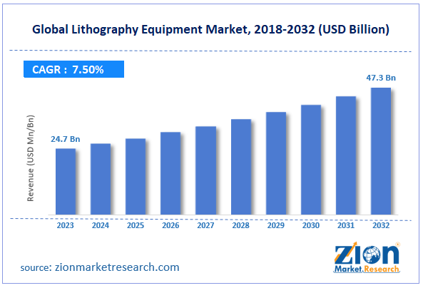
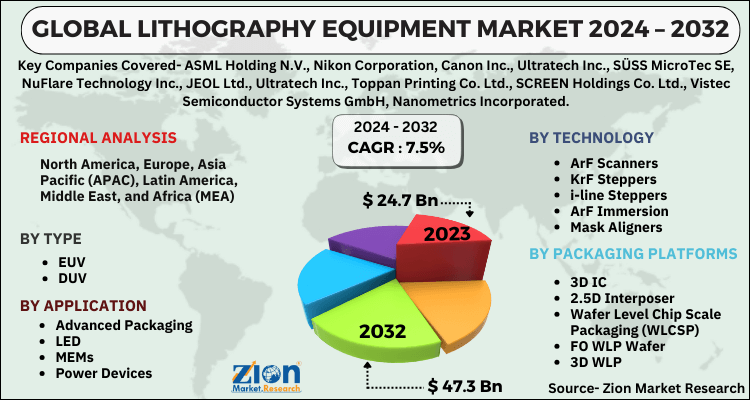
The global lithography equipment market size was worth around USD 24.7 billion in 2023 and is predicted to grow to around USD 47.3 billion by 2032 with a compound annual growth rate (CAGR) of roughly 7.5% between 2024 and 2032.
Lithography Equipment Market: Overview
Patterns for integrated circuits and semiconductor devices are designed using a collection of instruments known as lithography equipment. High-precision optics are necessary for lithography to focus radiation onto the exact areas of the wafer that will be exposed throughout the procedure. Using requests from a computer programmer, the patterning tool modifies light as it passes through lenses. The image is then projected onto the substrate using additional lenses or mirror systems. Before being exposed using lithography equipment onto a silicon substrate called a wafer, complex circuit patterns made on a huge glass photomask are shrunk in size using ultra-high-performance lenses.
Key Insights
- As per the analysis shared by our research analyst, the global lithography equipment market is estimated to grow annually at a CAGR of around 7.5% over the forecast period (2024-2032).
- In terms of revenue, the global lithography equipment market size was valued at around USD 24.7 billion in 2023 and is projected to reach USD 47.3 billion by 2032.
- The rising product launch is expected to drive the lithography equipment market over the forecast period.
- Based on the type, the EUV segment is expected to dominate the lithography equipment market over the forecast period.
- Based on the technology, the ArF Scanners segment is expected to hold the largest market share over the forecast period.
- Based on the application, the advanced packaging segment is expected to hold the largest market share over the forecast period.
- Based on the packaging platforms, the 3D IC segment is expected to dominate the market over the projected period.
- Based on region, Europe is expected to dominate the market during the forecast period.
Lithography Equipment Market: Growth Drivers
Rising demand for miniaturization drives market growth
Approximately 80% of contemporary automotive innovation is driven by the automobile industry, which uses electronic components that are essential for safety and are subject to high voltages and challenging climatic conditions. It is consequently required for manufacturers to develop new line semiconductors for automotive applications.
To keep up with the complexity of constructing safer, more eco-friendly, and intelligent automobiles, applications for intelligence, networking, sensing, and control are evolving quickly. Every new application demands advancements in the patterning technique used in semiconductor chip fabrication, which increases the overall use of semiconductors in today's high-tech automobiles. Thus, this is expected to drive the lithography equipment market during the forecast period.
Lithography Equipment Market: Restraints
Complexity in manufacturing process patterns hinders market growth
According to Moore's Law, density is the quantity of semiconductor chips packed into a specific 2D area. The cost of a chip is directly impacted by its area, so it must be taken into account. Some specialists believe that there is no more way to reduce the size of the semiconductor. Rapid size reduction raises design complexity and presents several manufacturing issues, even as it allows for faster processing and more economical power efficiency. The lithography process of semiconductors at such a small scale is limited by several variables.
One of the major challenges is handling complexity at the atomic level. Before the pattern is transferred from the photoresist to the wafer, the wafer's surface is either etched (material is removed) or has layers deposited in the lithography process. Section by section, the dopant materials are subsequently applied to the wafer in the pattern. It becomes very challenging to remove the created patterns at this stage without damaging the underlying wafer.
Lithography Equipment Market: Opportunities
Rising product launch offers a lucrative opportunity for market growth
The growing product launch is expected to offer a potential opportunity for industry expansion. For instance, in September 2024, the Texas Institute for Electronics (TIE), a semiconductor consortium based in Texas, received the FPA-1200NZ2C nanoimprint lithography (NIL) system, a lithography platform, from Canon Inc. With the debut of the FPA-1200NZ2C, Canon became the first company in the world to market a semiconductor manufacturing system that uses NIL technology, which produces circuit patterns in a different way than traditional projection exposure technology.
The novel product transfers a circuit pattern by pressing a mask imprinted with the circuit pattern into the resist on the wafer like a stamp, as opposed to traditional photolithography equipment that projects the circuit pattern onto the resist-coated wafer. Fine circuit patterns on the mask may be accurately replicated on the wafer because its circuit pattern transfer procedure does not include an optical mechanism. The new technique allows patterning with a minimum linewidth of 14 nm1, which is similar to the 5 nm node2 needed to make the majority of the most modern logic semiconductors now on the market while consuming less power and expense.
Lithography Equipment Market: Challenges
The high cost of advanced lithography equipment poses a major challenge to market expansion
Equipment used in lithography, particularly Extreme Ultraviolet (EUV) lithography, is very costly; each unit can cost hundreds of millions of dollars. For smaller semiconductor producers and foundries, the substantial initial expenditure needed for these systems is a major obstacle.
Manufacturers are burdened with high continuous operating and maintenance costs for lithography systems in addition to the initial purchase price. Therefore, the high cost of advanced lithography equipment poses a major challenge to the lithography equipment industry expansion.
Lithography Equipment Market: Report Scope
| Report Attributes | Report Details |
|---|---|
| Report Name | Lithography Equipment Market |
| Market Size in 2023 | USD 24.7 Billion |
| Market Forecast in 2032 | USD 47.3 Billion |
| Growth Rate | CAGR of 7.5% |
| Number of Pages | 212 |
| Key Companies Covered | ASML Holding N.V., Nikon Corporation, Canon Inc., Ultratech Inc., SÜSS MicroTec SE, NuFlare Technology Inc., JEOL Ltd., Ultratech Inc., Toppan Printing Co. Ltd., SCREEN Holdings Co. Ltd., Vistec Semiconductor Systems GmbH, Nanometrics Incorporated, Mapper Lithography, Neutronix Quintel Technology, Nanonex Corporation, EVG Group, Raith GmbH, NIL Technology, Orbotech, and others. |
| Segments Covered | By Type, By Technology, By Application, By Packaging Platforms, and By Region |
| Regions Covered | North America, Europe, Asia Pacific (APAC), Latin America, Middle East, and Africa (MEA) |
| Base Year | 2023 |
| Historical Year | 2018 to 2022 |
| Forecast Year | 2024 - 2032 |
| Customization Scope | Avail customized purchase options to meet your exact research needs. Request For Customization |
Lithography Equipment Market: Segmentation
The global lithography equipment industry is segmented based on type, technology, application, packaging platforms and region.
Based on the type, the global lithography equipment market is segmented into EUV and DUV. The EUV segment is expected to dominate the lithography equipment market over the forecast period. The resolution requirements of the semiconductor industry are too high for traditional Deep Ultraviolet (DUV) lithography, which is pushing for smaller node sizes (such as 5nm and 3nm). The need for EUV equipment is fueled by the fabrication of these smaller chips, which is made possible by EUV lithography's use of shorter wavelengths (13.5 nm).
Based on the technology, the global lithography equipment industry is bifurcated into ArF Scanners, KrF Steppers, i-line Steppers, ArF Immersion, Mask Aligners and Others. The ArF Scanners segment is expected to hold the largest market share over the forecast period. Features as small as 38–45 nm may be produced with it, and with other procedures, it can be extended to smaller sizes. This is necessary to produce more potent and effective chips and to stay up with Moore's law. This immersion lithography offers a good compromise between resolution, cost, and throughput because it has been tuned for high-volume manufacture. Because of this, it can be used to produce vast quantities of sophisticated microchips. As a result, this component speeds up market expansion.
Based on the application, the global lithography equipment market is bifurcated into Advanced Packaging, LED, MEMs and Power Devices. The advanced packaging segment is expected to hold the largest market share over the forecast period. Shorter interconnects between chips are made possible by this packaging, which lowers signal latency and boosts efficiency. Faster communication between processors is made possible by techniques like 2.5D and 3D stacking, which improve computing speed and energy efficiency. Additionally, by integrating several chips into a single device, these packaging approaches allow for greater capability in a smaller container. As a result, this element supports market expansion.
Based on the packaging platforms, the global lithography equipment industry is bifurcated into 3D IC, 2.5D Interposer, Wafer Level Chip Scale Packaging (WLCSP), FO WLP Wafer, 3D WLP and Others. The 3D IC segment is expected to dominate the market over the projected period. These three-dimensional integrated circuits (ICs) enable the vertical stacking of several circuit layers, increasing transistor density and performance. This increases the overall efficiency of lithographic equipment by allowing it to do more intricate calculations and control operations in a smaller space. Furthermore, makers of lithographic equipment can customize their systems to meet particular requirements because of the increased scalability and design freedom provided by 3D IC technology. As semiconductor production processes develop and demand increasingly sophisticated and adaptable solutions, this is very helpful. Thus, this element plays a role in market expansion.
Regional Analysis
Europe dominates the market over the projected period
Europe is expected to dominate the lithography equipment market during the forecast period. ASML, the world's top supplier of photolithography equipment, especially in the field of extreme ultraviolet (EUV) lithography, is based in the region. Europe is now a vital center for the advancement and uptake of cutting-edge lithographic technology due to ASML's dominance. With numerous colleges, research institutes, and commercial companies committed to developing semiconductor technology, it boasts a well-established research and development ecosystem. This R&D strength facilitates the creation and quick uptake of cutting-edge lithographic equipment. As a result, this factor accelerates the expansion of the global lithographic equipment market.
Lithography Equipment Market: Competitive Analysis
The global lithography equipment market is dominated by players like:
- ASML Holding N.V.
- Nikon Corporation
- Canon Inc.
- Ultratech Inc.
- SÜSS MicroTec SE
- NuFlare Technology Inc.
- JEOL Ltd.
- Ultratech Inc.
- Toppan Printing Co. Ltd.
- SCREEN Holdings Co. Ltd.
- Vistec Semiconductor Systems GmbH
- Nanometrics Incorporated
- Mapper Lithography
- Neutronix Quintel Technology
- Nanonex Corporation
- EVG Group
- Raith GmbH
- NIL Technology
- Orbotech
The global lithography equipment market is segmented as follows:
By Type
- EUV
- DUV
By Technology
- ArF Scanners
- KrF Steppers
- i-line Steppers
- ArF Immersion
- Mask Aligners
- Others
By Application
- Advanced Packaging
- LED
- MEMs
- Power Devices
By Packaging Platforms
- 3D IC
- 2.5D Interposer
- Wafer Level Chip Scale Packaging (WLCSP)
- FO WLP Wafer
- 3D WLP
- Others
By Region
- North America
- The U.S.
- Canada
- Europe
- France
- The UK
- Spain
- Germany
- Italy
- Rest of Europe
- Asia Pacific
- China
- Japan
- India
- South Korea
- Southeast Asia
- Rest of Asia Pacific
- Latin America
- Brazil
- Mexico
- Rest of Latin America
- Middle East & Africa
- GCC
- South Africa
- Rest of Middle East & Africa
Table Of Content
Methodology
FrequentlyAsked Questions
Patterns for integrated circuits and semiconductor devices are designed using a collection of instruments known as lithography equipment.
The lithography equipment market is being driven by several factors such as growing demand in several industries, technological advancement, rising product launch and increasing R&D investment by the key market players.
According to the report, the global market size was worth around USD 24.7 billion in 2023 and is predicted to grow to around USD 47.3 billion by 2032.
The global lithography equipment market is expected to grow at a CAGR of 7.5% during the forecast period.
The global market growth is expected to be driven by Europe. It is currently the world’s highest revenue-generating market due to the presence of major players and the growing product launch.
The global lithography equipment market is dominated by players like ASML Holding N.V., Nikon Corporation, Canon Inc., Ultratech Inc., SÜSS MicroTec SE, NuFlare Technology Inc., JEOL Ltd., Ultratech Inc., Toppan Printing Co. Ltd., SCREEN Holdings Co. Ltd., Vistec Semiconductor Systems GmbH, Nanometrics Incorporated, Mapper Lithography, Neutronix Quintel Technology, Nanonex Corporation, EVG Group, Raith GmbH, NIL Technology and Orbotech among others.
The market report covers the geographical market along with a comprehensive competitive landscape analysis. It also includes cash flow analysis, profit ratio analysis, market basket analysis, market attractiveness analysis, sentiment analysis, PESTLE analysis, trend analysis, SWOT analysis, trade area analysis, demand & supply analysis, Porter’s five forces analysis, and value chain analysis.
HappyClients
Zion Market Research
Tel: +1 (302) 444-0166
USA/Canada Toll Free No.+1 (855) 465-4651
3rd Floor,
Mrunal Paradise, Opp Maharaja Hotel,
Pimple Gurav, Pune 411061,
Maharashtra, India
Phone No +91 7768 006 007, +91 7768 006 008
US OFFICE NO +1 (302) 444-0166
US/CAN TOLL FREE +1 (855) 465-4651
Email: sales@zionmarketresearch.com
We have secured system to process your transaction.
Our support available to help you 24 hours a day, five days a week.
Monday - Friday: 9AM - 6PM
Saturday - Sunday: Closed


